Ultra-High Resolution & Ultra-High Sensitivity Scatterometer with Thin Film Measurement Capabilities
The n&k OptiPrime-X series are automated metrology systems used to fully characterize and monitor Thin Film and OCD applications for both current and next generation IC processes.
Utilizing patented all-reflective optics, a broadband wavelength range (190 – 1000nm), proprietary optical formulation, and an industry leading signal-to-noise ratio, each system provides the accurate and reproducible data required to monitor subtle changes in critical device parameters (thin film thickness, optical properties, critical dimensions (CD), poly recess profile, sidewall angle) across various key applications. The OptiPrime-X also incorporates a Single Wavelength ellipsometer to measure ellipsometric parameters at 633nm for added Thin Film Metrology capability.
High Throughput, Fully Automated Optical Metrology System for Higher Yields; with added 633nm Single Wavelength Ellipsometer for additional Thin Film R&R Capability
OptiPrime-X Series General Specifications
Wide Wavelength Range which allows for an extensive variety of applications
Film Thickness and Optical Properties
Trench/OCD Metrology Capabilities
Micro-Spot Technology
Configurable for all Wafer types and sizes
Full Automation that meets all Industry Fab and Foundry Standards
Easy to Maintain and Service
SEMI Standards and Third-Party Certifications
GEM/SECS Communication Interface
Thin Film & OCD Scatterometry Applications
Thin Film Application Examples
The n&k OptiPrime-X applications cover both current and next generation thin film measurement demands for R&D and Production: Ultra Thin Films and Residual Layers, Multi-Layer Stacks, Inhomogeneous Films, 193 nm and 248 nm ARCs and Resists, Low-κ Films, High-κ Films, and films deposited on practically any substrate. In addition, through the use of the SWE, the n&k OptiPrime-X offers excellent dynamic R&R results when measuring ultra-thin films.
DUV wavelengths are necessary in order to distinguish the ultra-thin HfO2 films
Measurement examples of HfO2 on a Si-Substrate demonstrates that the tool has plenty of sensitivity in the DUV for this measurement
Results of Analysis: — Bare Si, — 19.7Å HfO2 /Si, — 32.1Å HfO2 /Si,— 41.0Å HfO2 /Si
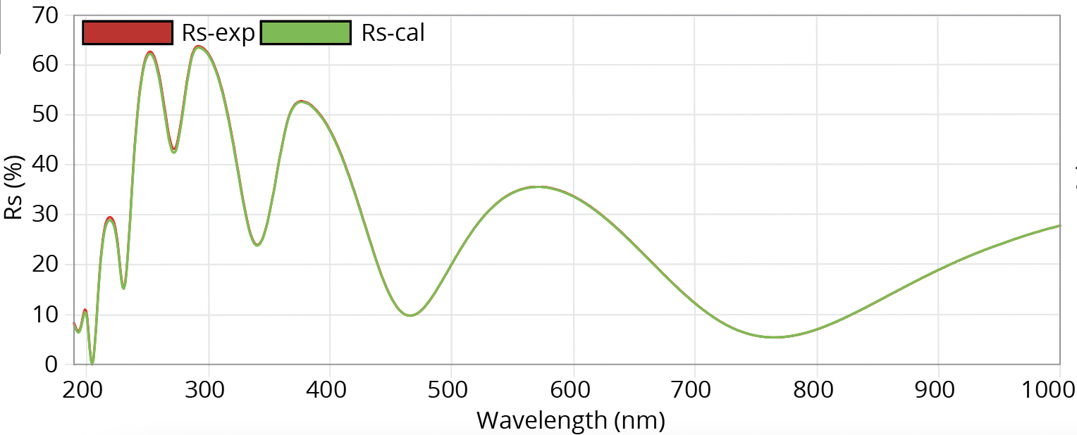
ADVANCED LITHOGRAPHY: RESIST / BARC / Si SUBSTRATE
Experimental and Calculated Reflectance Spectra
193 nm Resist = 2968 Å
193 nm BARC = 819 Å
Silicon Substrate
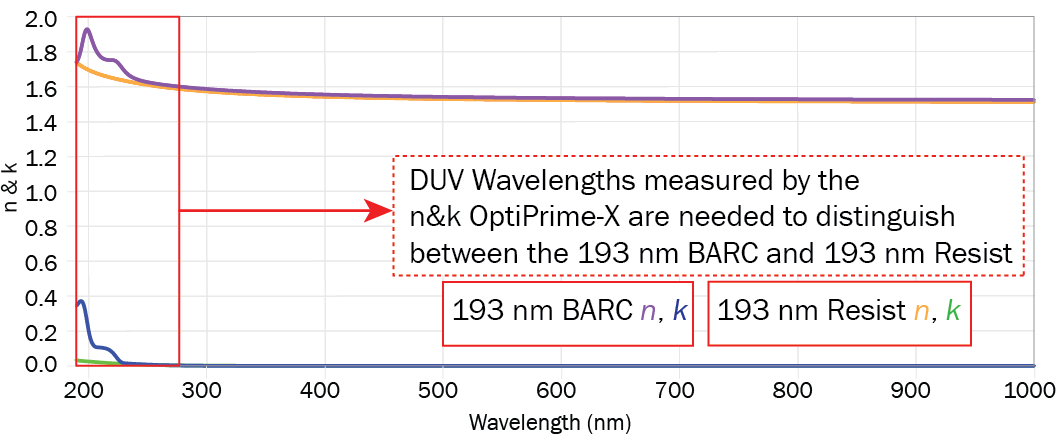
Results of Analysis: n and k Spectra of 193 nm BARC and Resist
Thicknesses and n and k spectra of 193 nm BARC and Resist are simultaneously determined:
Thickness Results: 193 nm Resist = 2968 Å 193 nm BARC = 819 Å
OCD Scatterometry Applications
The n&k OptiPrime-CD’s OCD scatterometry applications cover structures with very large pitches and very small pitches, 2-D and 3-D complex structures including films inside and outside of shallow and deep trenches and contact holes. Because of our patented and unique optical design, n&k Technology offers the highest signal-to-noise ratio and lowest cost of ownership to support your OCD requirement.
2-D COMPLEX STRUCTURE
n&k Results - Cross Sectional View
Experimental Spectra Showing Distinct Rs and Rp Polarized Spectra
3-D ASYMMETRIC ELLIPTICAL HOLES
n&k Results - Top View
Cross Sectional View
Experimental Spectra Showing Distinct Rs and Rp Polarized Spectra
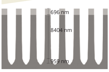
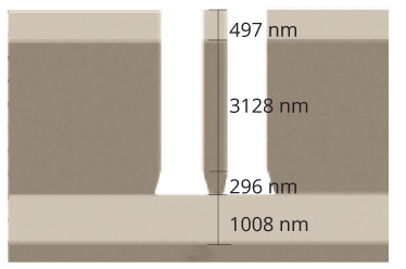
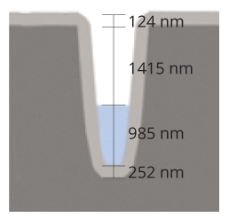
PROFILE COMPARISON WITH FIB AND X-SEM
Cross Section
n&k Results
SiO2 on Si Trench
SOI Trench (Flared CD Bottom)
Poly Recess Trench
n&k Technology OptiPrime-X Series Markets
Our products will be your eyes on the Nano scale, to ensure your IC’s and products have the highest yields.
Advanced Packaging
In addition to having our successes in the FEOL, we have now established success in the BEOL for various Advanced Packaging processes.
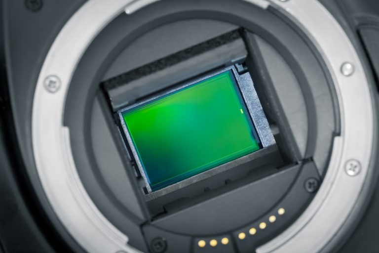
With the CMOS Image Sensor (CIS) market expected to grow significantly over the next several years, the rise in demand for image cameras for automotive, medical, and consumer goods will require high quality CIS devices.
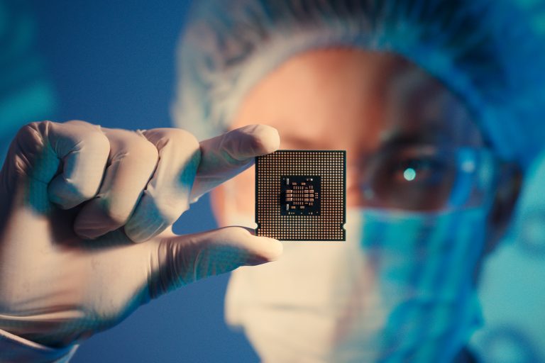
The foundation and building blocks of the electronics and computing industries, our products help ensure you can obtain the highest yields possible when manufacturing these integral IC’s.
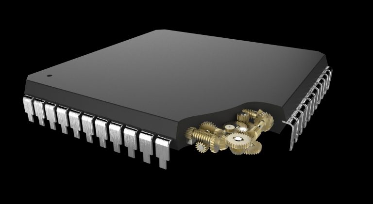
The world of MEMS manufacturing continues to grow as sensors, actuators, microvalves, and micropumps are rapidly produced due to their stellar device performance and low-cost levels.
Foundational in our technological eco-system in respect to electrical voltage and current flow, these devices are everywhere from the smallest consumer goods to the largest aircraft.