Olympian Series

Ultra-High Resolution &
Ultra-High Sensitivity Scatterometer
with Thin Film Measurement Capabilities
Based on DUV-Vis-IR Reflectometry

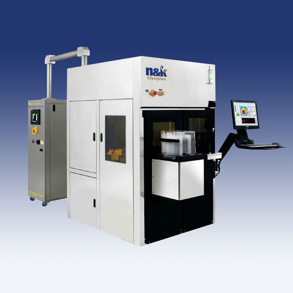
The n&k Olympian series are automated metrology systems used to fully characterize and monitor Thin Film and OCD applications for both current and next generation IC processes. Using an extended spectral range (190 – 15,000nm), the Olympian series monitors the widest array of Thin Film Applications (i.e., BPSG concentration, EPI-Si, SOI, etc.) and Trench/OCD Applications (High Aspect Ratio Structures) in the industry.

Utilizing patented all-reflective optics, a broadband wavelength range (190 – 15,000nm), proprietary optical formulation, and an industry leading signal-to-noise ratio, each system provides the accurate and reproducible data required to monitor subtle changes in critical device parameters (thin film thickness, optical properties, critical dimensions (CD), poly recess profile, sidewall angle) across various key applications.

Streamline Applications in a Non-Destructive Manner from an SEM, FTIR, Reflectometer, Ellipsometer, CD-SEM, AFM, Profiler – All with one Olympian system

Olympian Series General Specifications

  • Widest Wavelength Range in the Industry which allows for an extensive variety of applications
  • Film Thickness and Optical Properties
  • Trench/OCD Metrology Capabilities  
  • Micro-Spot Technology
  • Configurable for all Wafer types and sizes
  • Full Automation that meets all Industry Fab and Foundry Standards
  • Easy to Maintain and Service
  • SEMI Standards and Third-Party Certifications
  • GEM/SECS Communication Interface

Thin and Thick Film & OCD Scatterometry Applications

Due to their ability to measure a large range of OCD and thin film structures that cover current and future applications, the tools belonging to the Olympian Series are used extensively for the most challenging applications of today’s semiconductor industry.

Thin and Thick Film Application

The n&k Olympian’s thin and thick film applications cover both current and next generation measurement demands for R&D and production: Ultra-Thin Films and Residual Layers, Multi-Layer Stacks, Inhomogeneous Films, 193 nm & 248 nm ARCS and Resists, Low-κ films, High-κ films, films deposited on Rough Surfaces, EPI Film Stacks, and Ultra-Thick Resists.

Ultra-Thick Film Measurement
SOI Schematic
~30 μm of Si - The Device Layer
~1 μm of SiO2 - The BOX Layer
Si Substrate

Experimental reflectance spectra in the IR region measured at three different locations. Low frequency interference fringes are due to BOX thickness; high frequency interference fringes are due to Si device layer thickness.

Device Layer Uniformity Plot (nm)
-8 -6 -4 -2 0 2 4 6 8 8 6 4 2 0 -2 -4 -6 -8 31300 31100 Mean 30200 30000

Device Layer Thickness Results (nm):
Max = 31285
Mean = 30902
Min = 30069
Std Dev = 254

Box Layer Uniformity Plot (nm)
-8 -6 -4 -2 0 2 4 6 8 8 6 4 2 0 -2 -4 -6 -8 1015 1000 Mean 950 935

Box Layer Thickness Results (nm):
Max = 1014
Mean = 985
Min = 941
Std Dev = 16.3

Epi Silicon Measurement
Epi Silicon Schematic
Epi Silicon
Si Substrate

Experimental reflectance spectra in the IR region measured for three different Epi-Si/Si samples.
The frequency of interference fringes relates to the Epi-Si thickness.

OCD Scatterometry Applications

The n&k Olympian’s OCD scatterometry applications cover structures with very large and very small pitches, 2-D and 3-D complex structures with high & low aspect ratios, and structures with films inside and outside of trenches and contact holes.

DEEP 3-D STRUCTURE
Structure Information
Contact Hole Depth: 10 – 20 μm
Oxide Thickness: ~1 μm
X-Pitch: 2 μm
Contact Hole Diameter: ~1 μm
Top View Schematic
2 μm ~1 μm
Cross Section Schematic
SiO 2 2 μm ~15 μm ~1 μm ~1 μm Si
600 700 800 900 0 5 10 15 20 25 30 35 40 R (%) Wavelength (nm) 500 Wafer Top: 1270 nm SiO 2 Wafer Center: 1278 nm SiO 2 Wafer Bottom: 1270 nm SiO 2 1000

Experimental Spectra: In the Vis-NIR range, the shift of the interference fringes occurs because of the variation in the mesa SiO2 thickness. No variation due to the changes in contact hole depth is observed in this wavelength range.

15 20 25 30 35 40 45 50 5000 5500 6000 6500 7000 7500 8000 R (%) Wavelength (nm) Wafer Top: 11.46 µm Hole DepthWafer Center: 11.70 µm Hole DepthWafter Bottom: 11.54 µm Hole Depth 55 4500 8500 10

Experimental Spectra: In the IR range, the shift of the interference fringes occurs because of the variation in the trench depth. The frequency of the interference fringes at the center of the wafer has the largest value. Therefore, the contact holes at the center are the deepest of the three.

Role of UV-Vis-NIR and IR Measurements for OCD Applications
DEEP TRENCHES IN Si WITH OXIDE
Deep Trenches in Si with Oxide SEM vs. n&k Results

n&k Technology Olympian Series Markets

Our products will be your eyes on the Nano scale, to ensure your IC’s and products have the highest yields.

Advanced Packaging

In addition to having our successes in the FEOL, we have now established success in the BEOL for various Advanced Packaging processes.

Automotive

Sensors, safety features, advanced braking technology, auto-pilot driving; these technologies all require advanced Automotive IC’s.

Image Sensor

With the CMOS Image Sensor (CIS) market expected to grow significantly over the next several years, the rise in demand for image cameras for automotive, medical, and consumer goods will require high quality CIS devices.

Foundry/Logic/Memory

The foundation and building blocks of the electronics and computing industries, our products help ensure you can obtain the highest yields possible when manufacturing these integral IC’s. 

MEMS

The world of MEMS manufacturing continues to grow as sensors, actuators, microvalves, and micropumps are rapidly produced due to their stellar device performance and low-cost levels.

Power Device

Foundational in our technological eco-system in respect to electrical voltage and current flow, these devices are everywhere from the smallest consumer goods to the largest aircraft.

Specialty IC

Bridging the digital and physical worlds, Specialty IC’s supplement Logic technology, creating a new wave of technological innovation. 

Malcare WordPress Security