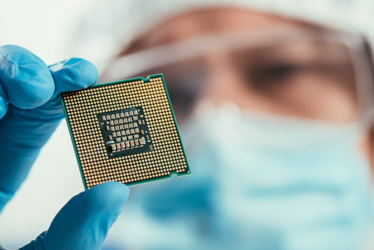
n&k Technology’s optical metrology systems for Thin Film and Trench/OCD applications are Field-Proven to monitor all facets of daily critical processing steps for various technological manufacturing needs.
Field Proven & Production Worthy Optical Metrology
Our systems offer experimental data with the highest signal-to-noise ratio over the widest wavelength range in the industry. As a result, the critical information you obtain using the n&k systems leads to higher yields.
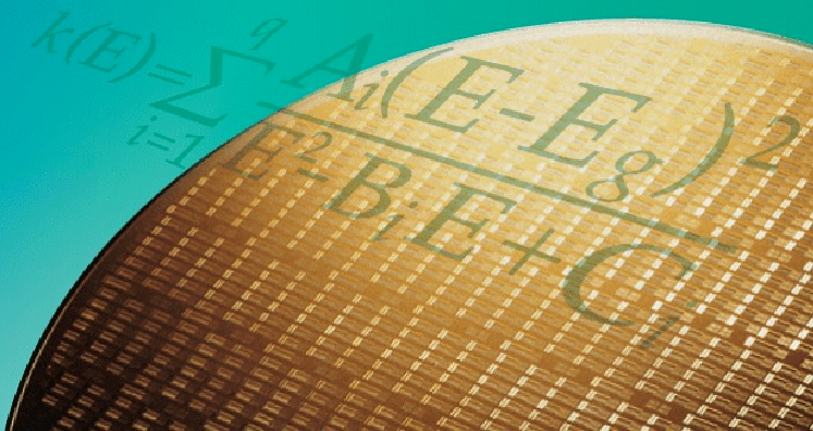
Analysis is based on the Forouhi-Bloomer dispersion equations, which are valid physical models that enable the n&k systems to monitor the most challenging current and next generation IC processes.
n&k Technology’s optical metrology systems for Thin Film and Trench/OCD applications are Field-Proven to monitor all facets of daily critical processing steps for various technological manufacturing needs.
Field Proven & Production Worthy Optical Metrology
Our systems offer experimental data with the highest signal-to-noise ratio over the widest wavelength range in the industry. As a result, the critical information you obtain using the n&k systems leads to higher yields.
Analysis is based on the Forouhi-Bloomer dispersion equations, which are valid physical models that enable the n&k systems to monitor the most challenging current and next generation IC processes.
Patented Technology that Enables Process Control and Yield Improvement of Devices Comprising Thin Films, Trenches and Contact Holes
Thin Film
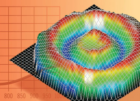
n&k’s thin film measurement systems accurately and repeatably determine thicknesses, n and k spectra, and energy band gap (Eg) of ultra-thin films (e.g. mono-layer graphene) and ultra-thick films (e.g. Epi-Si) for single-layer or multi-layer film stacks. Films can be characterized on either rough or smooth substrates.
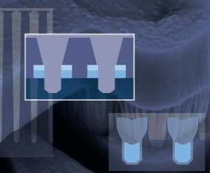
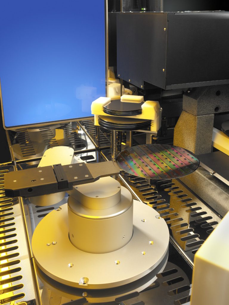
n&k’s scatterometers accurately and repeatably determine Depth, CD, and Profile of complex 2D (trenches) and 3D (contact holes) IC structures. Whether the structure has a small pitch (<0.5µm), large pitch (>10µm), or high-aspect ratio, n&k systems can detect subtle changes in critical device parameters (including hardmask and sidewall oxide thicknesses).
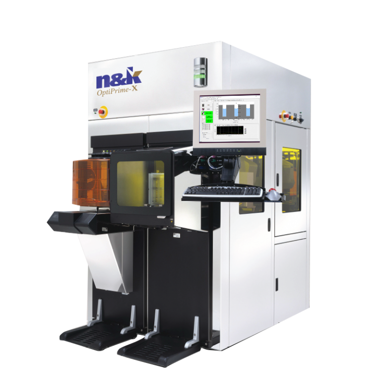
The core technology is based on DUV-Vis-NIR (or IR) broadband reflectance (and transmittance for transparent substrates). n&k systems utilize patented all-reflective optics to achieve optimal signal-to-noise ratio of raw data which is then analyzed with the Forouhi-Bloomer Dispersion Equations combined with Rigorous Coupled Wave Analysis to monitor the most critical parameters.
We Listen and Understand the needs of our partners to push technological barriers.
We Innovate and manufacture cutting edge optical metrology products.
Our products Enable our partners to produce IC’s that help power the world and humanity.
Why People Trust Us
n&k Technology’s Scatterometers and Thin Film Metrology Tools are.
Yield-Enhancing
The ability to quickly measure multiple dies per wafer results in higher-quality IC products and increased overall yield.
Production-Worthy
Fully automated; meets all automation requirements present in today’s most advanced fabs and foundries.
Field Proven
Installed in high volume production fabs and foundries worldwide for over two decades.
Non-Destructive
Eliminate the need to scrap wafers for SEM, which in-turn, will speed up your ROI.
Fast
Optical metrology allows for immediate feedback at multiple locations enabling significantly high throughput compared to traditional metrology techniques.
The accuracy, speed & ease-of-use of the n&k analyzer was far superior to standard ellipsometry. Quite frankly, I don’t know of any other machine which can provide so much information, so accurately and so quickly.
What I really like about the n&k system is its very powerful engine but at the
same time it’s very user friendly. The technical support from n&k is great when something does go wrong, which is rare, as good as the machine is.
RTC recently bought a 1512-RT n&k tool for phase, transmission, reflectivity,
and resist thickness measurements and it’s a great tool. Greg Hughes, Jeff
Myron, and myself have all worked with it recently and can’t say enough good
things about it.
Thank you for your e-mail. I’m also thanking your company and all members of your company. It’s no problem to write about our experience of your RT system, because I personally think that your system was greatly helpful in my research and to our company.
Faculty and students at Fudan University are making extensive use of the n&k 8000 for thin film measurements and also when conducting research, writing technical papers and theses. Thank you very much for your support.
A CD measurement with the n&k analyzer provides a high throughput,
non-destructive and accurate method for the determination of the critical dimensions and depths of periodic structures like trenches and resist gratings.
The True Measure
The technology which we help enable is a part of our daily lives. No matter where you look, what you touch, or which device you use; our products are a helping hand in building our digital world.
We have a saying here at n&k – “If you can make it, we can measure it.” We also like to add that even if you can’t make it, we can probably still measure it.
As the world continues to utilize technology to push new boundaries, we will continue to stay at the forefront of technology by committing to Listen, Understand, Innovate, and Enable our customers.
n&k’s unique combination of hardware + software allows for the monitoring of the most critical thin film & scatterometry applications.
Experimental data with the highest signal-to-noise ratio over the widest wavelength range in the industry
Analysis of measured data based on valid physical models – Forouhi Bloomer Dispersion Equation and RCWA