Ultra-High Resolution & Ultra-High Sensitivity Scatterometer and Thin Film Measurement System for Photomask or Semiconductor Wafer Applications
The n&k Gemini series are automated metrology systems used to fully characterize and monitor Thin Film and OCD applications for both current and next generation IC processes. Capable of simultaneous Reflectance and Transmittance measurements the Gemini series is ideal for applications with transparent substrates (i.e., Photomasks, SiC Wafers, Quartz Wafers, Flat Panels, etc.).
Utilizing patented all-reflective optics, a broadband wavelength range (190 – 1000nm), proprietary optical formulation, and an industry leading signal-to-noise ratio, each system provides the accurate and reproducible data required to monitor subtle changes in critical device parameters (thin film thickness, optical properties, critical dimensions (CD), poly recess profile, sidewall angle) across various key applications.
High Throughput, Fully Automated Optical Metrology System for Higher Yields for either Opaque or Transparent Substrates.
Gemini Series General Specifications
Wide Wavelength Range which allows for an extensive variety of applications
Film Thickness and Optical Properties
Trench/OCD Metrology Capabilities
Micro-Spot Technology
Configurable for all Wafer types and sizes
Full Automation that meets all Industry Fab and Foundry Standards
Easy to Maintain and Service
SEMI Standards and Third-Party Certifications
GEM/SECS Communication Interface
Thin Film & OCD Scatterometry Applications
Photomask Application Examples
CONVENTIONAL MASK - THIN FILM
To characterize the mask film stack shown on the right, three spectra are measured: Frontside R, Frontside T, and Backside R.
The measured spectra are then fitted simultaneously using the Forouhi-Bloomer Dispersion equations to determine the thickness and n and k of all layers.
MoSi Uniformity
Cr Uniformity
CrOx (ARC) Uniformity
Photoresist Uniformity
n and k Spectra of Cr:
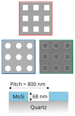
OPTICAL CRITICAL DIMENSION (OCD)
In this example application, the desired measurement output is the degree of rounding of contact holes in MoSi on quartz.
The figure on the right shows the sensitivity of the raw reflectance and transmittance data to corner rounding. The high sensitivity of the transmittance data allows for accurate measurements of this quantity. Also note the high level of the transmittance (65% at 800 nm) compared to the reflectance (15% at 800 nm). This high level improves the signal-to-noise and hence the repeatability of the measurement.
This example illustrates the importance of the n&k Gemini’s unique transmittance capability in achieving accurate and repeatable results.
Measurements of Corner Rounding:
Sensitivity of Rp & Tp
PHASE SHIFT
As critical dimensions (CD) become smaller, mask manufacturers increasingly use phase shift technologies to enhance the resolution of the resist image that is formed on the wafer
Frontside Measurement
Backside Measurement
The n&k Gemini determines phase shift from 190-1000 nm through R and T measurements and through the analysis of film optical properties, film thickness and quartz etch depth.
EUV LITHOGRAPHY
The n&k Gemini can measure structures used in EUV lithography, as well as the thickness and n and k spectra of the associated materials.
Using measurements on blanket areas, the thicknesses and n and k spectra can be found for:
Superstructure Multi-layer Mo and Si
Capping and buffer layers
Absorber materials
ARC materials
OCD MEASUREMENTS OF EUV MASK
For OCD applications, the depth, CD and sidewall angle of the arc/absorber buffer layer structure can be measured.
The high speed of measurement (~5 seconds per point) allows for detailed uniformity maps to be obtained.
Example: Depth Uniformity Map
Example: CD Uniformity Map
Semiconductor Wafer Application Examples
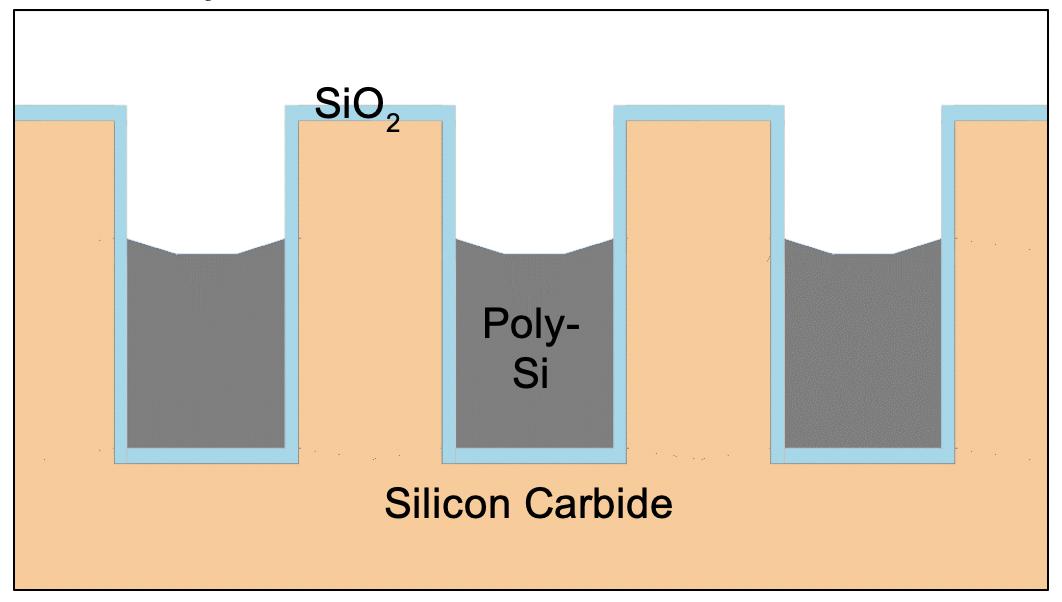
Poly Recess measurements can be done for Silicon Carbide, with similar capabilities to Silicon devices
Recess Depth, CD and SiO2 Thickness can be measured
Poly Recess in SiC
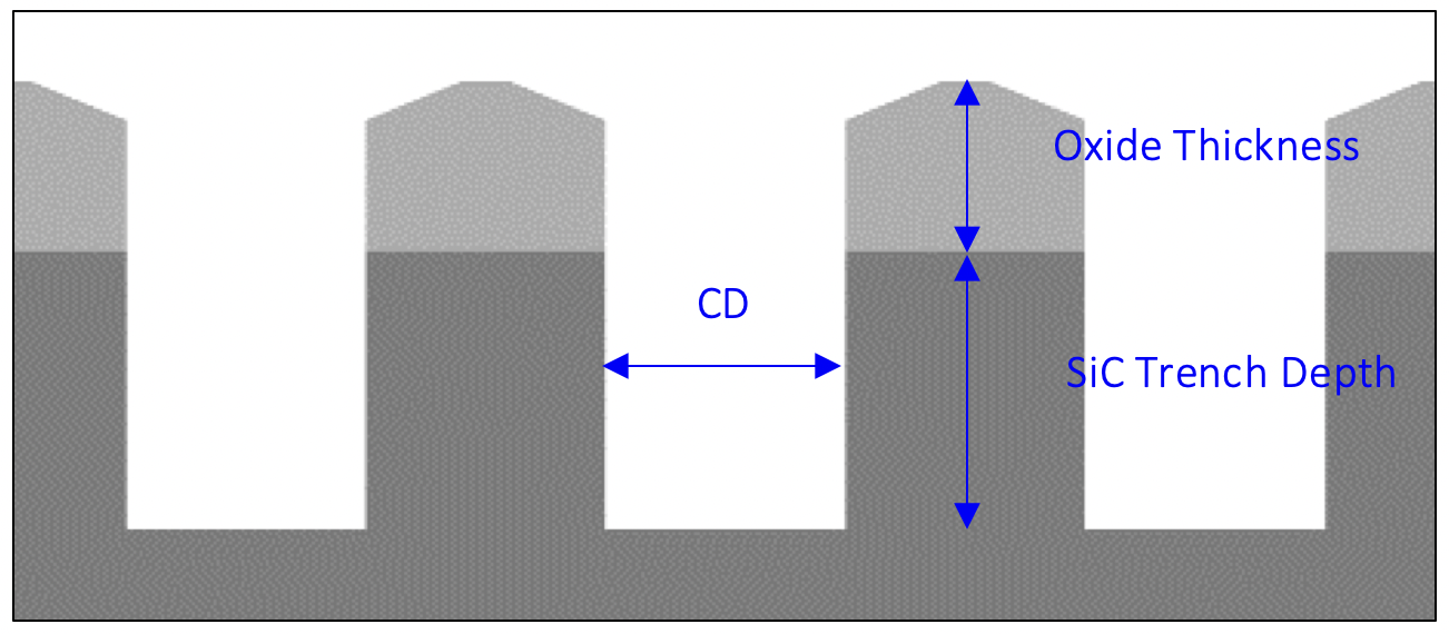
Trenches in SiC
Using the combination of reflectance and transmittance, accurate and repeatable results can be obtained for trenches in SiC.
We can measure trench depth, Oxide thickness, and CD for the structures with 2µm pitch and 6µm pitch
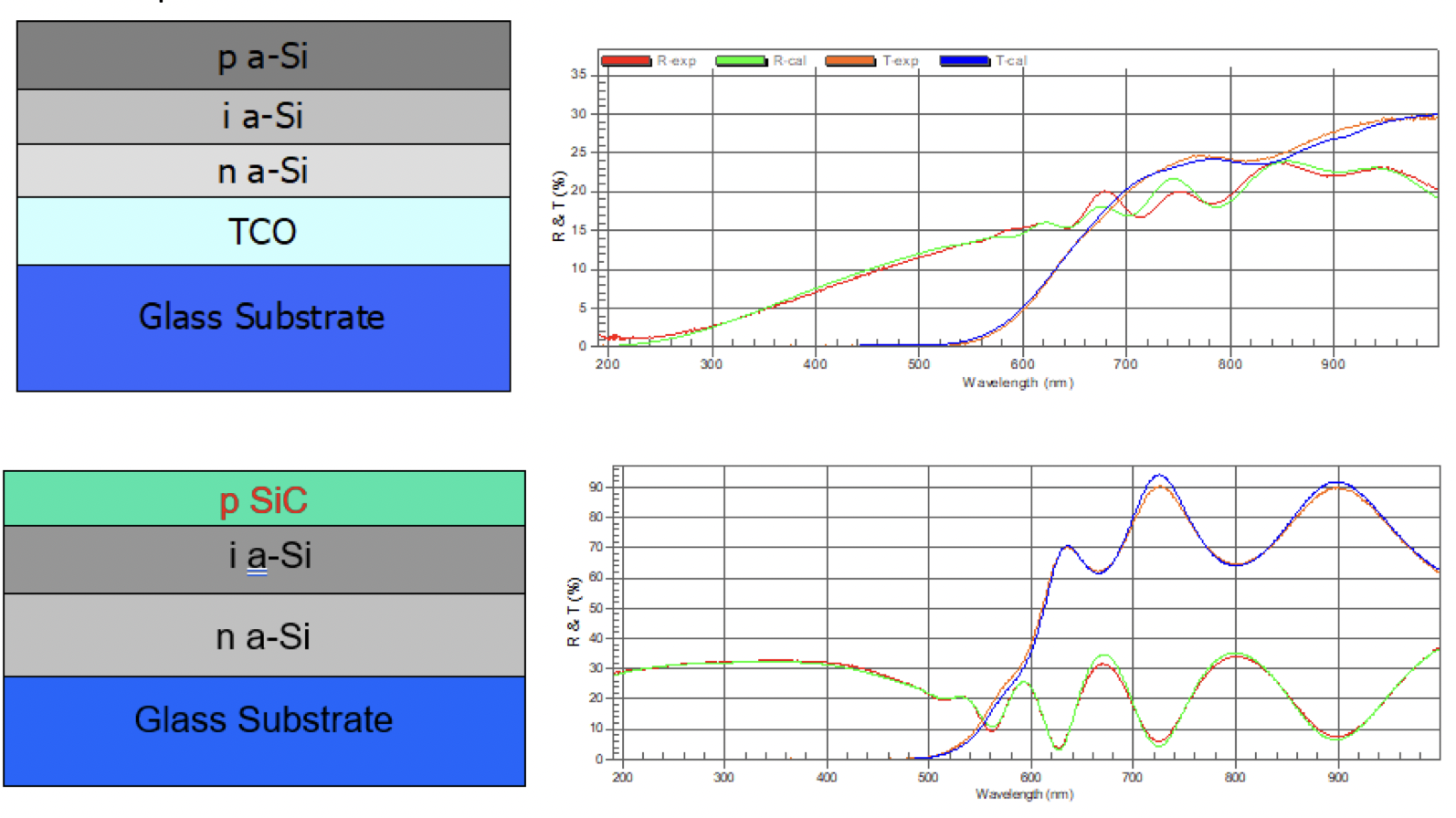
SOLAR EXAMPLE
n&k is capable of monitoring multilayer thin films on “p-i-n” solar cells
Through the use of both Transmittance and Reflectance, n&k can characterize the thickness and optical properties of the various layers in the solar cell.
IMPRINT LITHOGRAPHY
Template
Media Processing
Media Final Product
Typical top views for the above profiles:
n&k Technology Gemini Series Markets
Our products will be your eyes on the Nano scale, to ensure your IC’s and products have the highest yields.
Flat Panel Display
Displays continue to play a part of everyday life by way of smartphones, tablets, TV’s and monitors. Our products continue to enable the display manufacturers to produce high quality displays at the highest yield possible.
Optical metrology for Conventional, Phase Shift, or EUV photomasks remains key for Photomask shops worldwide. Our unique combination offering to measure both Reflectance and Transmittance has proven to be very beneficial to Photomask makers throughout the years.
Foundational in our technological eco-system in respect to electrical voltage and current flow, these devices are everywhere from the smallest consumer goods to the largest aircraft.